Organization chart of the service
Introduction to the service
APC's Electronics and Microelectronics Department comprises thirteen people, including five research engineers, five design engineers, two assistant engineers and one technician. It is involved in the laboratory's flagship space, land and underwater projects.
The department is equipped with a full range of CAD (Computer Aided Design) tools for the design of specific integrated circuits (ASICs) and printed circuit boards (PCBs), as well as electronic and microelectronic simulation tools.
The department produces several studies a year of varying size and complexity, from double-sided PCBs to 12-layer PCBs with microvias, from class 4 to non-class 88 μm. Manufacturing is subcontracted. The department is responsible for editing the manufacturing follow-up file, requesting quotes and generating the files required by the subcontractor, which are then sent to the designers.
A wiring workshop enables the production of prototypes, which can be wired either manually or using a rewiring oven. This workshop can also be used to replace defective components.
The department manages the “low noise” room, a Université Paris Cité platform integrated into the Pôle Spatial Paris-Cité, dedicated to the testing and characterization of temperature-controlled low-frequency reading and detection chains.
The department's electronics engineers design, build, test and monitor systems destined to operate on experimental sites in often harsh environments (ionizing radiation, extreme temperatures and pressures, vibrations, etc.). For these reasons, the various projects we carry out are subject to strict quality criteria. The department's engineers also take on project management responsibilities at both national and international level. They apply project management principles based on space methodology, integrating product assurance and quality control aspects right from the early stages of project development.
Expertise
The systems designed by the department call on a wide range of electronic skills: fast analog, low-noise and high-dynamic, and digital, and use a variety of technologies: discrete components, bipolar or CMOS integrated circuits, analog, digital or mixed, programmable or specific. Programmable digital circuits (FPGAs) programmed in VHDL or VERILOG are widely used.
The microelectronics activity is organized around three permanent research engineers and one design engineer, supported by the laboratory's IT department for maintenance of the necessary CAD resources. Circuits are designed on a full-custom basis using standard CADENCE Virtuoso tools. Most developments have been carried out using AMS CMOS and BiCMOS SiGe 0.35µm technologies, as well as STMicroelectronics BiCMOS SiGe 130nm technology.
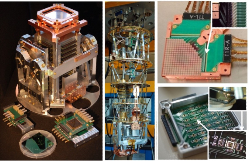
The department has developed specific expertise in the design of low-noise ASICs (below nV/sqrt Hz), operating in cryogenic environments (4K) for the integration of superconducting sensors (TES, SQUID, KIDS) or hardened in radiative environments for space applications. This expertise was key to the development of the bolometric interferometer for the QUBIC ground-based telescope (cryogenic readout chain), dedicated to millimeter-wave observation of the polarization of the cosmic microwave background (CMB), and to the readout chain for the X-IFU (warm front-end electronic) instrument on board the ATHENA space mission satellite, for the observation of high-energy phenomena in the X range.
The department also specializes in the development of very low-noise digital and analog electronic systems deployed for the detection of gravitational waves.
