APC's microelectronics department develops ASICs (Application Specific Integrated Circuit) for the implementation of instruments dedicated to observational cosmology and astroparticle experiments.
Team presentation :
This service consists of two permanent research engineers: Fabrice Voisin, who has been in office since 2003, currently head of the microelectronics department, part of the QUBIC and WFEE ATHENA projects; Damien Prêle, in office since 2007, attached to the QUBIC project and project manager WFEE ATHENA.
In September 2015, Cyril Beillimaz joined the service, benefiting from a CDD funded by CNES to carry out Phase A of the WFEE ATHENA project. Since September 2016, Si Chen, doctoral student co-supervised by Damien Prêle, is also involved in the development of integrated circuits within the framework of this same project.
Expertise field :
APC's microelectronics department has full-custom design capabilities from ASIC's front-end analog and mixed-mode ASICs using standard CMOS and BiCMOS technologies for applications at ambient temperature or at very low temperatures.
In particular, the members of this department have developed a specific expertise within the IN2P3 for the design of ultra-low-noise (0.2 nV / √Hz) ASICs, In a cryogenic environment (4.2 K) for the integration of superconducting (TES, SQUID) or hardened sensors to radiative environments for space applications.
Over the past five years, the department has also participated in the development of Single Photon Avalanche Diode (SPAD) matrices for the production of single photon sensitive imagers using standard CMOS ASIC technology.
Projects:
QUBIC (Q & U Bolometric Interferometer for Cosmology):
The R & D department has developed expertise in the area of SQUID (Superconducting QUANTUM Interference Device) time division multiplexers for the reading of large Transition Edge matrices -Sensors) using ultra-low-noise integrated circuits operating at cryogenic temperature.
This solution, developed in particular in the context of BSD R & D, is particularly innovative for instruments dedicated to observational cosmology that integrate ultra-sensitive complex cryogenic detection systems and which require a high rate of multiplexing.
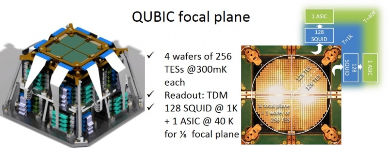
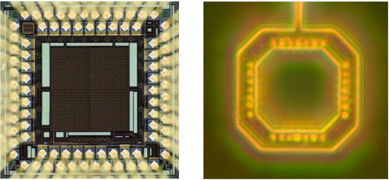
Two ASICs were carried out, one in 2012 ("SQMUX128") for the integration and validation of one quarter of the QUBIC detection chain in a dilution cryostat (2015) and the second one in 2016 ("SQMUX128_evo" In order to equip the demonstrator of the final instrument in its dedicated cryostat (2017). It is in this context that the microelectronics service has taken charge of the realization and qualification of the ASICs equipping the cryogenic detection chain of the telescope QUBIC (two focal planes of 1024 TES each), international experiment of ground interferometry in the field of millimeter and submillimetric waves (150 GHz and 220 GHz) for the study of cosmic diffuse polarization B modes (CMB for Cosmic Microwave Background).
These ASICs implement a time division multiplexing of 4 columns of 32 SQUIDs in series for the reading of 128 TESs. They incorporate an ultra-low noise amplifier (0.2 nV / √Hz) with 4 multiplexed inputs, 32 multiplexed current sources required for SQUID polarization, a digital circuit for addressing sequencing and a serial link to parameterize The entire circuit.

In addition to the production of these ASICs operating at cryogenic temperature (4.2 K), the microelectronics department is largely involved in the integration of the instrument detection chain: definition and characterization of TES (300 mK superconducting detectors) ; Specification, implementation follow-up and testing of SQUID (superconducting preamplifier at 1 K); Realization and integration of SQUID and ASIC modules (PCB); Interconnection management (bonding, cables and connectivity); Specification and interfacing of the hot acquisition electronics (300 K).
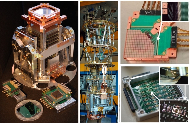
These ASIC implementations operating at very low temperatures were proposed in the framework of an international collaboration with the PMO Institute (Purple Mountain Observatory, China) for the implementation of the focal plane of a telescope located at Dôme A in Antarctic. In 2013, the microelectronics department realized, tested and provided the collaboration with a new ASIC ("SQMUX24") integrating the functionalities necessary for the reading and the time multiplexing of 24 TES. A second ASIC is being prepared for 2017 to equip the final 1024 TES instrument.

ATHENA (Advanced Telescope for High Energy and Astrophysics):
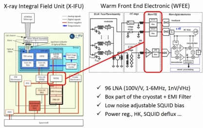
In the framework of the ATHENA space observatory in the field of X-rays, ESA mission L2, the APC is responsible for the WFE (Warm Front End Electronic) subsystem of the X-IFU instrument on board the satellite .
The focal plane of the X-IFU detector is composed of 3840 TES, the signals of which are frequency-multiplexed with a rate of 40, ie a number of channels to be amplified and then reduced to 96.
The main function of the WFEE, located at the interface of the cryostat and the DRE (Digital Readout Electronic), is to integrate the 96 channels of amplification (ultra-stable gain 100V / V , 1 - 6MHz, 1nV / √Hz) and as many adjustable current sources (DAC in current) required for the polarization of the SQUIDs present in the cryogenic stages as well as an I2C or RS485 serial link for the parameterization of the " together.
The project is currently in phase A for a satellite launch scheduled for 2028.
A first ASIC ("awaXe_v1") was submitted to the foundry at the beginning of 2016, including numerous test vehicles in order to identify the topologies compatible with WFEE requirements and to validate the radiation hardening techniques used for the Realization of digital cells.
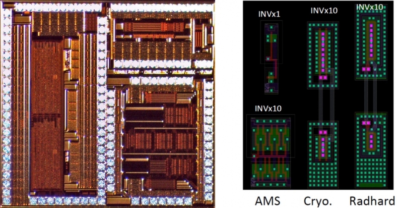
The microelectronics department also supported the ASIC characterization phases, including a qualification campaign in radiation resistance (dose and beam), as well as the development of associated PCBs and test benches.
These radiation dose tests (source at Cobalt 60 on the COCASE, CEA Saclay site) and in a bundle (Californium 252 source at the TRAD facility and at the UCL Louvain cyclotron) Microelectronics to have undeniable competence in space qualification.

A second ASIC ("awaXe_v2") is being developed for submission at the end of 2017 for a "breadboard" integration for the implementation of a demonstrator scheduled at the end of phase A (2018).
The microelectronics department participated in the development of Single Photon Avalanche Diode (SPAD) matrices in standard ASIC CMOS technology for the production of single photon sensitive imagers in the Gamma Cube, R & D for spatial gamma tracker project. The study of an integrated coding and multiplexing system leads to the realization, in 2014, of an ASIC ("IMACUP") in the framework of an academic collaboration with LE2I (Electronic, Computer and Image Laboratory). The service also supported the characterization of this multiplexed SPAD matrix as well as the implementation of the associated test bench.
Future projects:
The microelectronics service is designed to meet the demands of projects emerging in the laboratory requiring its expertise. In this capacity, he is actively participating in the future prospects for contributions to the LiteBird satellite project and to the project of the fourth generation S4 American instrument for the study of the CMB or its European equivalent E4.