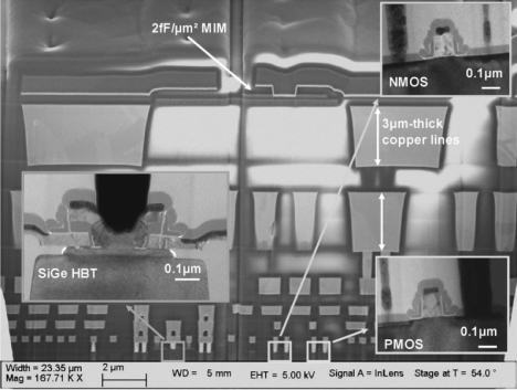


The BiCMOS R&T is a transverse IN2P3 project coupled with an alternative technology work package WP1.1 of MI2I. In its current form, it is intended to compare the BiCMOS technologies currently available.
Indeed, as the noise and gain efficiency performances are very high on bipolar technologies, the R&T aims at establishing and comparing merit factors (such as gm/Ic, gmRout, gmfroutT, √Si_C ...).
Future IN2P3 experiments have a strong need for front-end analogue. ASIC design is evolving towards more and more digital, justifying the use of full CMOS technology. In order to keep technologies able to respond to analogue performances coupled to a specific detector, it is important to keep at least one mature BiCMOS and general purpose technology. Indeed, many medical nuclear physics detectors need dynamics rather than integration density. Astronomical instruments need low noise readings down to very low frequencies, which is not compatible with the low frequency noise feedback of MOS transistors.
Technologies of interest
- TSMC 130
- AMS 350
- IHP 130 SG13S – R&T
- IHP 250
- TSI 180
- ON SEMI 350
- ST 9MW SiGe 130nm - APC
- XFAB 180nm CMOS ou SOI – R&T
Objectives
- To identify a "sustainable" and affordable technology that can meet a wide range of needs in analogue (and somewhat mixed) front-end electronics, with a moderate number of channels.
- Create synergy around this technological node.
- Rationalise ASIC developments in the space, astro, nuclear and medical fields.


